

Our Fabrication Laboratory

Creating Excellence with Quality and Reliability
In the semiconductor industry, fabrication labs are the facilities where devices are created and tested for quality and reliability. Fabrication labs, or otherwise known in the semiconductor industry as "Cleanrooms" are the backbone of the industry. On this page, we explain in depth what the industry standards of cleanrooms are and their importance in the semiconductor industry.
We do not outsource to third Parties for Quality Control

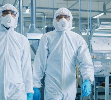
When clients require the services of semiconductor companies, one of the biggest challenges is attaining high-quality work. Part of quality control is the physical facility in which the devices are developed. At Zener Engineering, we design and develop in a Class 1000 cleanroom, to ensure quality standards are followed, plus we do front-to-backend product development, with testing, reliability, and packaging, all at our facility for a complete customer service experience.
What is a Class 1000 Cleanroom?
A Class 1000 cleanroom, also called ISO 6 in the semiconductor industry, is defined as one that limits airborne particles to 1000 (≥0.5 µm) particles per cubic foot of air. To achieve this, advanced air filtration is used with HEPA filters, with at least 180 air changes required per hour, producing a 20%-30% filter coverage. In addition to air filtration, the temperature, humidity ranges, along with strict personnel protocols, are adhered to with specialized materials to prevent contamination.
To further elaborate on cleanrooms, the greater the number of particles in a cleanroom, the greater the number of airborne particles will be. For example, an engineering company offering services, claiming they have a 10,000k cleanroom, means that the number of airborne particles will be 10x greater than a Class 1000 cleanroom, where there are only 1000 airborne particles per cubic foot of air. A higher percentage of particles per cubic foot of air increases the probability of contamination, such as rusting and mold. This will result in sub-standard quality of devices, with short-circuiting taking place.
Key Characteristics & Requirements of Class 1000 Cleanrooms

-
Particle limits: A maximum of 1,000 particles per cubic meter of air that are 0.5μm0.5 mu m
0.5𝜇𝑚 or larger.
-
Air filtration: Utilizes HEPA (High-Efficiency Particulate Air) or sometimes ULPA (Ultra-Low Penetration Air) filters to remove contaminants.
-
Air changes: Requires at least 180 air changes per hour.
-
Filter coverage: The filtration system must cover 20-30% of the room's area.
-
Airflow: Often uses unidirectional (laminar) airflow to maintain cleanliness, which is more efficient than turbulent airflow.
-
Temperature and humidity control: The temperature is typically maintained between 64−68∘F64 minus 68 raised to the composed with power cap F64−68∘𝐹 (18−20∘C18 minus 20 raised to the composed with power cap C
18−20∘𝐶) and humidity between 35-40% to protect sensitive components from static electricity and moisture.
-
Specialized materials: Floors, walls, and ceilings are made from smooth, non-shedding, and easy-to-clean materials like static-dissipative vinyl or stainless steel.
-
Personnel protocols: Requires strict gowning procedures for all personnel entering the room, including coveralls, hairnets, and masks, to prevent contamination from the human body.
-
Equipment and layout: Equipment like lighting and electrical outlets are often installed in a way that prevents them from trapping dust and other particles, typically on the ceiling or upper walls
What is a Cleanroom Used for in the Semiconductor Industry?

Cleanrooms are the backbone of the semiconductor industry. Cleanrooms are the facilities that finally bring to fruitation the devices ordered by clients. Without cleanrooms, there can be no implementation of the devices that took months or even years of collaboration between engineering companies and clients. Here are some of their common uses in the industry:
-
Assembly and testing: Used for complex microelectronic assemblies such as surface-mount technology (SMT).
-
Wire bonding: A process that connects wires to electronic components, requiring a high level of cleanliness.
-
Die attach: The process of bonding a semiconductor die to a substrate.
-
Flip chip underfill: Used in the process of underfilling a flip chip with an epoxy.
-
Prototyping: Suitable for prototyping and commercialization of miniature electronic products where cleanliness is critical.