

Heterogeneous Integration
Heterogeneous Integration
Heterogeneous Integration.... Advanced Package Engineering for The Next Level

Chiplets
Chiplets are small, modular semiconductor chips designed to perform a specific function, such as processing, a memory block, an I/O driver, or a signal processing unit. Several or unlimited chiplets can be incorporated into a single die, to create a truly complex system that disaggregates a monolithic chip into smaller, functional blocks, allowing designers to mix and match different components like CPUs, GPUs, and memory from various vendors to create a tailored system for a specific application. This modular design improves manufacturing yields, lowers costs, and accelerates innovation compared to traditional, single-chip designs monolithic microchip, taking a chip's capabilities to new heights.

Interposers
An interposer is an intermediate layer in an IC package that sits between an IC substrate and two or more chips. This component provides signal routing, power distribution, and even thermal management for the IC dice in the package. Inteposers can be made in various materials such as silicon, organic, and glass, with each offering its unique advantages, making them suitable for different applications in IC packaging. Some of the modern areas that leverage interposers are high-performance computing, consumer electronics, and mil-aero and military embedded systems.
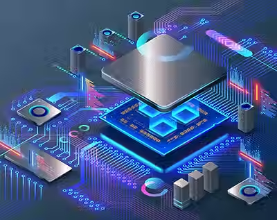
Hetrogeneous intergration in the semiconductor is truly like a work of art. It is the technology of combining multiple specialized, separately manufactured chips (chiplets) into a single package to create a more powerful and functional system. Instead of a single large, monolithic chip, it uses advanced packaging techniques like 2.5D/3D-IC integration and Through-Silicon Via (TSV) to connect these smaller components, which can be made using different process technologies. This approach improves performance, power efficiency, and yield while also lowering costs and accelerating time-to-market.

Through-Silicon Vias
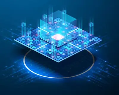
Through-Silicon Vias (TSVs) are vertical, electrical connections that run completely through a silicon wafer or die, enabling 3D stacking and direct interconnection of multiple semiconductor chips. This technology creates more compact and higher-performance systems by replacing traditional 2D connections with a more efficient 3D architecture, used in applications like GPUs, AI processors, and data center chips
TSV fabrication can fall into three methods depending on how the via is constructed—via-first, via-middle and via-last. For example, the via-first process involves creating a deep via in the silicon from the top of the wafer followed by a reveal process that exposes the backside of the wafer. These vias can be a few microns in diameter and are very large and have high aspect ratios compared to the other features of integrated circuits. They need longer processing times and the fabrication process is quite complex.
Key Characteristics & Advantages of Heterogeneous Integration
Embedded Multi-Die Interconnect
Embedded multi-die interconnect bridge (EMIB) is a technology that uses that uses small, embedded silicon pieces to connect multiple chips (chiplets) within a single package. They provide high-density, high-bandwidth interconnects between dies that are fabricated on different process nodes, making them ideal for heterogeneous integration and a more cost-effective alternative to large silicon interposers.
EMIB's are more cost-effective than large silicon interposers because it only uses silicon for the areas that need high-density connections, not the entire interposer.
In addition to being more cost-effective, EMIB's also offer more mechanical reliability. Embedding reduces mechanical stresses on semiconductor dies by eliminating traditional wire bonding, which can be a common point of failure due to vibration and thermal cycling. Enhanced mechanical robustness makes embedded power modules ideal for harsh environments such as automotive, aerospace, and industrial applications.
Benefits of Heterogeneous Integration
Advanced Package Engineering Solutions That Deliver Results
At Zener Engineering, our goal is not just to provide services to semiconductor companies, but to bring back the technologies that have largely been outsourced and left US shores many years ago. Advanced Package engineering is one of those technologies, with very little being offered within the United States now, and we here at Zener Engineering believe in also being informative to let our clients know all the advantages and benefits these technologies have to offer. Heterogeneous Integration (HI), being an integral part of advanced package engineering design, offers the following benefits:
-
Improved yield: Smaller chiplets have lower defect rates, leading to higher overall yields.
-
Performance: Chiplets can be optimized for their specific function, leading to better power efficiency and speed.
-
Cost reduction: It allows for the use of more expensive, advanced process nodes only where they are needed, while other functions can use more mature, cost-effective nodes.
-
Flexibility and speed: Faster time-to-market because designers can mix and match different chiplets more easily