


Wafer-Level Packaging
Wafer-Level Packaging

Cutting Edge Technology With Pace with Efficiency
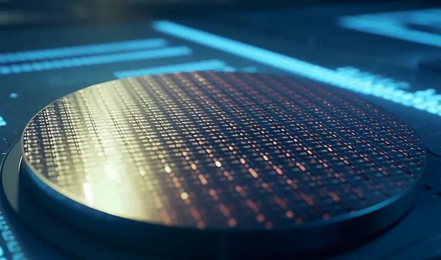
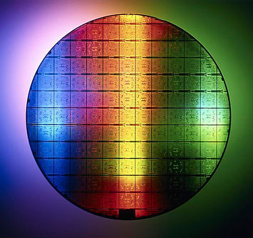
Wafer-lever packaging is a semiconductor IC technology that involves the process of attaching components to an integrated circuit (IC) directly at the wafer level before the wafer is sliced, as opposed to the conventional method of assembling and packaging each individual die separately. This technology streamlines production for devices that are smaller and thinner, at a rapid pace, while at the same time harnessing the most cutting-edge technology to boost efficiency at every turn. Wafer-level packaging's demand rose in response for more powerful CPU's and to meet the high volume of production needed for devices such as smartphones, smart devices and Internet of Things (IoT).
What is Wafer-Level Packaging?

Packaging With Cost and Release to Market Solutions
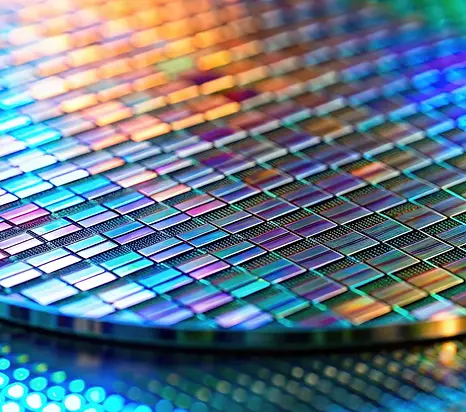
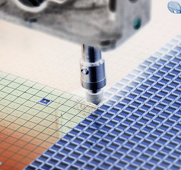
Industries that produce products on a mass scale, such as smartphones, smart devices, Internet of Things (IoT), and sensors, need to not only be able to get things to the market in as little time as possible, but retain cost and efficiency with precision, and Wafer-Level Packaging has been the solution of choice. The reason for this is that wafer-level packaging is crucial in enhancing the overall performance of electronic devices while simultaneously reducing manufacturing costs and minimizing space requirements, since packaging is applied on whole wafers and wafers are diced only after the packaging is successfully completed. In wafer-level packaging, the components used in assembly, such as bumps, are applied at the wafer level, prior to dicing. In traditional semiconductor manufacturing, the wafers are first diced into separate dies and are then assembled into a semiconductor package such as QFN or BGA.
In addition to the small size and low cost benefits, Wafer-Level Packaging offers integration of wafer fabrication and testing, at the wafer level, resulting in a more streamlined manufacturing process, simplifying the journey a device undertakes from the silicon base to the finished shippable customer product.
Types of Wafer-Level Packaging
Packaging Solutions with Variety
Fan-Out Wafer-level Packaging
-
Embedding the die: A chip is embedded in a mold compound, which provides a base for the subsequent layers.
-
Redistribution Layer (RDL): A thin-film redistribution layer is built over the molded die and the surrounding area to create new, finer traces. These traces connect the original chip pads and extend outward, hence "fanning out".
-
External connections: The RDL is then topped with solder balls, which serve as the external connections for the package.
-
No traditional substrate: Unlike some other packaging methods, FOWLP eliminates the need for a traditional substrate, which can reduce costs and improve electrical performance
-
Higher I/O count: It overcomes the limitation of traditional WLP by allowing the number of external connections to exceed the original die size.
-
Improved performance: Shortening interconnect lengths leads to lower signal delay and better electrical performance.
-
Miniaturization: The ability to eliminate substrates and create smaller packages supports the development of more compact electronic devices.
-
Increased design flexibility: The fan-out RDLs provide more space for routing, offering greater design freedom
There are two main types of Wafer-Level Packaging; namely, Fan-In Wafer-Level Packaging (FIWLP) and Fan-Out Wafer-Level Packaging (FOWLP). Both types of packaging use an interposer, which provides the electrical connection between the die and components in a package. The main difference is the level of the interposer. In a Fan-Out wafer, the interposer is the same size as the die, whereas in Fan-Out wafer, the interposer is larger than the die, similar to conventional BGA packages.
What differentiates FOWLP and FIWLP from Ball Grid Array (BGA) packages is the fact that the interposer is applied directly on the wafer in the case of the WLP package, instead of making use of the flip-chip technique, whereas the Ball Grid Array die is attached and reflowed to the interposer. In both FIWLP and FOWLP packages, the die and the interposer can be encapsulated in a protective material, such as epoxy or thermo-resistant plastics.
Key Characteristics and Advantages of Fan-In & Fan-out Wafer-Level Packaging
Fan-In Wafer-level Packaging
-
Compact size: The final package is the same size as the chip itself, making it ideal for devices where space is limited.
-
Cost-effective: It is a cost-efficient process as it uses existing fabrication tools and requires fewer steps than other packaging methods.
-
High-frequency applications: The short electrical paths can lead to higher radio-frequency (RF) performance.
-
No interposer: Unlike some other advanced packaging, it does not require a separate interposer to connect the die to the package
-
Process Efficiency: FI-WLP is highly cost-effective and streamlines manufacturing by integrating wafer fabrication, testing, and packaging at the wafer level, eliminating the need for traditional single-die assembly processes like wire bonding or interposers.
-
Packaging at the wafer level: Instead of dicing chips first, the packaging process is done while the chips are still on the wafer.
-
Redistribution layer (RDL): A redistribution layer is used to fan the I/Os out from their original location on the die to a larger, more suitable area on top of the die.
-
Bumping: The I/Os are then connected to solder bumps, which are the "balls" of the ball-grid array, at the new, larger locations.
-
Chip-scale package: This process creates a true Chip-Scale Package (CSP) because the resulting package is the same size as the original die
Benefits of Wafer-Level Packaging
Wafer-Level Packaging...Cost, Efficiency and Quality....In One
Wafer-level Packaging offers a wide range of benefits that make it an ideal choice in semiconductor manufacturing, offering improved electrical and thermal performance, and cost reduction due to processing the entire wafer before dicing. It enables smaller, more powerful, and more energy-efficient devices by shortening signal paths, improving heat dissipation, and simplifying manufacturing processes, which is crucial for the development of compact electronic devices.
Benefits of Wafer-Level Packaging
Performance & Efficiency
-
Miniaturization: WLP creates ultra-thin and compact packages, which is essential for devices like smartphones and wearables.
-
Enhanced electrical performance: Shorter electrical paths reduce parasitic capacitance and inductance, leading to faster signal transmission and improved signal integrity.
-
Improved thermal management: The technology enhances heat dissipation because the package is in closer proximity to the silicon, and some WLP techniques help spread heat more efficiently.
-
Lower power consumption: Faster signal speeds and reduced resistance can lead to lower overall power consumption
Manufacturing & Cost
-
Streamlined manufacturing: Packaging, testing, and burn-in can be integrated at the wafer level, simplifying the overall manufacturing process.
-
Cost-effectiveness: Economies of scale from wafer-based processes and fewer manufacturing steps can lead to lower production costs, especially for high-volume production.
-
Improved reliability: WLP can reduce the potential for defects often introduced during traditional assembly processes
Design & Integration
-
Smaller footprint: WLP reduces the size and mass of components, making it easier for designers to create more functional devices in smaller form factors.
-
System-in-package (SiP) integration: The scalability of WLP allows for combining multiple dies and components without wire bonds, enabling advanced SiP solutions